1. Material Residences and Structural Integrity
1.1 Intrinsic Features of Silicon Carbide
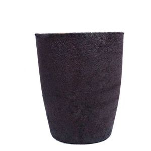
(Silicon Carbide Crucibles)
Silicon carbide (SiC) is a covalent ceramic compound made up of silicon and carbon atoms arranged in a tetrahedral latticework framework, mostly existing in over 250 polytypic kinds, with 6H, 4H, and 3C being the most technically pertinent.
Its strong directional bonding imparts outstanding hardness (Mohs ~ 9.5), high thermal conductivity (80– 120 W/(m · K )for pure single crystals), and outstanding chemical inertness, making it among one of the most robust materials for severe atmospheres.
The broad bandgap (2.9– 3.3 eV) guarantees excellent electrical insulation at space temperature and high resistance to radiation damage, while its reduced thermal growth coefficient (~ 4.0 × 10 ⁻⁶/ K) contributes to exceptional thermal shock resistance.
These innate buildings are protected even at temperature levels surpassing 1600 ° C, enabling SiC to maintain architectural honesty under extended exposure to molten metals, slags, and reactive gases.
Unlike oxide ceramics such as alumina, SiC does not react readily with carbon or kind low-melting eutectics in minimizing environments, a critical advantage in metallurgical and semiconductor processing.
When fabricated right into crucibles– vessels designed to consist of and warmth products– SiC outperforms conventional materials like quartz, graphite, and alumina in both lifespan and procedure integrity.
1.2 Microstructure and Mechanical Security
The performance of SiC crucibles is very closely connected to their microstructure, which depends on the production technique and sintering additives utilized.
Refractory-grade crucibles are commonly generated using response bonding, where permeable carbon preforms are penetrated with liquified silicon, creating β-SiC via the response Si(l) + C(s) → SiC(s).
This procedure produces a composite structure of primary SiC with residual free silicon (5– 10%), which boosts thermal conductivity but may restrict usage over 1414 ° C(the melting factor of silicon).
Additionally, completely sintered SiC crucibles are made through solid-state or liquid-phase sintering making use of boron and carbon or alumina-yttria ingredients, accomplishing near-theoretical thickness and higher pureness.
These exhibit exceptional creep resistance and oxidation stability but are much more expensive and tough to make in large sizes.
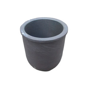
( Silicon Carbide Crucibles)
The fine-grained, interlacing microstructure of sintered SiC supplies outstanding resistance to thermal tiredness and mechanical erosion, crucial when dealing with molten silicon, germanium, or III-V substances in crystal development processes.
Grain boundary design, consisting of the control of secondary phases and porosity, plays an important function in figuring out long-lasting sturdiness under cyclic heating and hostile chemical atmospheres.
2. Thermal Performance and Environmental Resistance
2.1 Thermal Conductivity and Heat Distribution
One of the specifying advantages of SiC crucibles is their high thermal conductivity, which makes it possible for quick and uniform warmth transfer during high-temperature processing.
Unlike low-conductivity materials like integrated silica (1– 2 W/(m · K)), SiC efficiently disperses thermal energy throughout the crucible wall, decreasing localized hot spots and thermal gradients.
This uniformity is essential in procedures such as directional solidification of multicrystalline silicon for photovoltaics, where temperature level homogeneity straight influences crystal top quality and flaw density.
The combination of high conductivity and reduced thermal development causes a remarkably high thermal shock parameter (R = k(1 − ν)α/ σ), making SiC crucibles resistant to breaking during rapid heating or cooling cycles.
This permits faster heating system ramp rates, improved throughput, and reduced downtime because of crucible failure.
In addition, the product’s capability to hold up against repeated thermal cycling without significant deterioration makes it excellent for set processing in industrial heaters running above 1500 ° C.
2.2 Oxidation and Chemical Compatibility
At elevated temperatures in air, SiC undergoes easy oxidation, creating a protective layer of amorphous silica (SiO TWO) on its surface: SiC + 3/2 O ₂ → SiO ₂ + CO.
This lustrous layer densifies at heats, working as a diffusion barrier that reduces more oxidation and maintains the underlying ceramic structure.
Nonetheless, in reducing environments or vacuum problems– typical in semiconductor and steel refining– oxidation is reduced, and SiC continues to be chemically stable versus liquified silicon, aluminum, and many slags.
It withstands dissolution and response with molten silicon up to 1410 ° C, although prolonged exposure can lead to slight carbon pick-up or user interface roughening.
Most importantly, SiC does not present metal pollutants into sensitive thaws, an essential demand for electronic-grade silicon manufacturing where contamination by Fe, Cu, or Cr needs to be maintained listed below ppb degrees.
However, care should be taken when processing alkaline planet steels or very reactive oxides, as some can corrode SiC at severe temperatures.
3. Manufacturing Processes and Quality Control
3.1 Construction Strategies and Dimensional Control
The production of SiC crucibles entails shaping, drying, and high-temperature sintering or seepage, with methods picked based on needed pureness, dimension, and application.
Common developing methods consist of isostatic pressing, extrusion, and slip casting, each providing different degrees of dimensional precision and microstructural harmony.
For big crucibles used in photovoltaic ingot spreading, isostatic pushing guarantees regular wall surface thickness and density, reducing the threat of crooked thermal development and failure.
Reaction-bonded SiC (RBSC) crucibles are affordable and commonly used in shops and solar industries, though recurring silicon limitations optimal service temperature level.
Sintered SiC (SSiC) variations, while much more expensive, offer remarkable pureness, stamina, and resistance to chemical attack, making them ideal for high-value applications like GaAs or InP crystal development.
Accuracy machining after sintering might be required to achieve tight resistances, specifically for crucibles used in upright slope freeze (VGF) or Czochralski (CZ) systems.
Surface area ending up is vital to decrease nucleation websites for issues and guarantee smooth thaw circulation during casting.
3.2 Quality Control and Performance Validation
Extensive quality assurance is important to make certain dependability and durability of SiC crucibles under requiring operational problems.
Non-destructive examination methods such as ultrasonic testing and X-ray tomography are utilized to find interior fractures, gaps, or thickness variants.
Chemical analysis using XRF or ICP-MS verifies low levels of metal pollutants, while thermal conductivity and flexural toughness are measured to confirm product uniformity.
Crucibles are frequently subjected to simulated thermal biking tests before shipment to identify possible failing settings.
Set traceability and qualification are typical in semiconductor and aerospace supply chains, where part failure can bring about expensive manufacturing losses.
4. Applications and Technical Influence
4.1 Semiconductor and Photovoltaic Industries
Silicon carbide crucibles play a pivotal function in the production of high-purity silicon for both microelectronics and solar batteries.
In directional solidification heaters for multicrystalline photovoltaic or pv ingots, large SiC crucibles work as the key container for liquified silicon, sustaining temperatures over 1500 ° C for numerous cycles.
Their chemical inertness protects against contamination, while their thermal stability makes sure consistent solidification fronts, bring about higher-quality wafers with less dislocations and grain borders.
Some producers layer the internal surface area with silicon nitride or silica to better reduce attachment and facilitate ingot launch after cooling down.
In research-scale Czochralski growth of compound semiconductors, smaller SiC crucibles are utilized to hold thaws of GaAs, InSb, or CdTe, where minimal reactivity and dimensional security are vital.
4.2 Metallurgy, Foundry, and Arising Technologies
Past semiconductors, SiC crucibles are essential in metal refining, alloy prep work, and laboratory-scale melting procedures involving aluminum, copper, and rare-earth elements.
Their resistance to thermal shock and disintegration makes them suitable for induction and resistance heating systems in foundries, where they last longer than graphite and alumina options by numerous cycles.
In additive manufacturing of responsive metals, SiC containers are made use of in vacuum induction melting to avoid crucible breakdown and contamination.
Arising applications include molten salt activators and focused solar energy systems, where SiC vessels may contain high-temperature salts or fluid metals for thermal power storage.
With continuous advancements in sintering technology and finish engineering, SiC crucibles are positioned to support next-generation materials processing, enabling cleaner, extra effective, and scalable commercial thermal systems.
In recap, silicon carbide crucibles stand for an essential allowing innovation in high-temperature product synthesis, integrating outstanding thermal, mechanical, and chemical efficiency in a solitary crafted component.
Their prevalent adoption across semiconductor, solar, and metallurgical sectors underscores their role as a keystone of contemporary commercial ceramics.
5. Distributor
Advanced Ceramics founded on October 17, 2012, is a high-tech enterprise committed to the research and development, production, processing, sales and technical services of ceramic relative materials and products. Our products includes but not limited to Boron Carbide Ceramic Products, Boron Nitride Ceramic Products, Silicon Carbide Ceramic Products, Silicon Nitride Ceramic Products, Zirconium Dioxide Ceramic Products, etc. If you are interested, please feel free to contact us.
Tags: Silicon Carbide Crucibles, Silicon Carbide Ceramic, Silicon Carbide Ceramic Crucibles
All articles and pictures are from the Internet. If there are any copyright issues, please contact us in time to delete.
Inquiry us